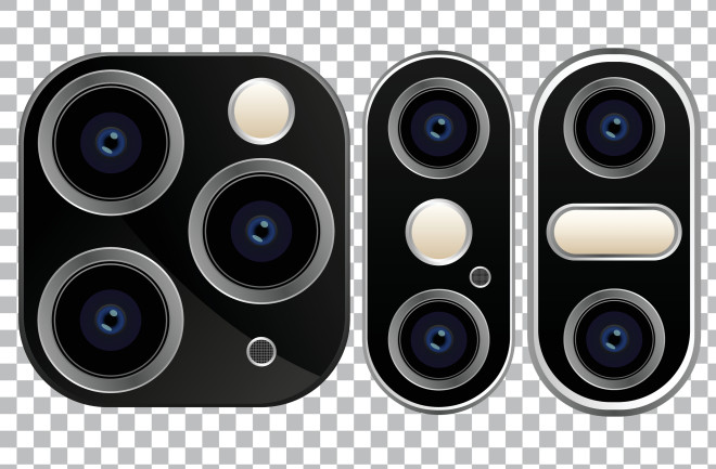
One of the more expensive parts of the cameras built-in to smartphones is the lens system. That’s because lenses have to be made in an entirely different way to the electronic components that make up the rest of the phone.
In recent years, physicists have hoped to change this with a new type of “metalens” that can be carved onto a flat sheet of silicon dioxide or similar material. Metalenses consists of pillars of silicon that are each about the same size as the wavelength of light.
These pillars interact with light, causing it to bend and scatter in precisely controllable ways. So by arranging large numbers of pillars in periodic arrays, physicists can make them bend light in the same way as a conventional lens.
That paves the way for metalenses to be etched onto the same silicon chips that are otherwise used for capturing and processing images. In this scenario, expensive conventional lenses become entirely obsolete.
Faltering Efforts
But attempts to create metalenses using light-based lithography have so far faltered.
What’s needed is another way to make metalenses that is compatible with the large-scale manufacture of chips.
Enter Andrew McClung and colleagues at the University of Massachusetts in Amherst, who have demonstrated exactly this — a new way to make metalenses that is compatible with chip manufacture. They say their approach “has potential for widespread adoption in consumer electronics and imaging systems.”
Conventional lenses are generally made by pouring glass or plastic into a mold and then grinding and polishing it into the required shape. If used in a mobile phone or similar imaging system, these lenses then have to be carefully aligned with the chip and glued into place. That’s fiddly, complicated and expensive.
In the last decade, physicists have begun making metalenses using a process called electron beam lithography, which can carve tiny features onto substrates. But because electrons are difficult to control, this process is not suitable for large-scale chip manufacture. This generally relies on light-based lithography, which cannot yet make metalenses at the required scale.
So instead of conventional optical lithography, McClung and co have perfected essentially the opposite technique. Instead of carving the pattern onto a substrate, they imprint it, a bit like stamping a pattern into a clay tablet.
This technique, called nanoimprint lithography, begins by casting a nanoscale stamp made of a silicon polymer. They then press this stamp into a synthetic resin called polymethyl methacrylate or PMMA. This resin sits on top of a layer of silicon nitride on top of a layer of silicon dioxide.
Print Charming
This imprinting process leaves a pattern in the shape of the metalens that can then be etched onto the substrate. The result is a pattern of silicon nitride pillars sitting on top of the silicon dioxide substrate — a metalens.
McClung and co show how this technique can create lenses 6mm in diameter that accurately focus visible light to near the diffraction limit and with a focusing efficiency of 81 per cent. By comparison, a similar lens they made using electron beam lithography achieved focusing efficiency of 89 per cent.
That’s interesting work that has the potential to be used in current mass production facilities. “The scalable fabrication of high efficiency metasurfaces operating in the visible wavelength range opens up opportunities for their widespread adoption in consumer applications,” say the researchers.
Cameras in smartphones, webcams, and the like, are only a few of these applications. Metalenses can also be used to channel light through chips, creating complex 3D designs for processing light. “This advancement enables the development of highly efficient and compact optical systems that can be seamlessly integrated into various applications,” say McClung and co.
If they are right, metalenses should be coming to a smartphone near you soon (ish)!
Ref: Visible metalenses with high focusing efficiency fabricated using nanoimprint lithography : arxiv.org/abs/2312.13851

